Semiconductor manufacturing process flow
2026/6/18
The semiconductor manufacturing process mainly includes the following steps:
Wafer preparation: Single crystal silicon is extracted from high-purity silicon, cut into wafers, and cleaned and polished to ensure a smooth surface.
Oxidation: Forming a thin layer of silicon dioxide on the wafer surface that acts as an insulating layer.
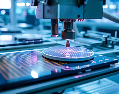
Photolithography: Transferring circuit patterns onto a wafer using photolithography technology.
Etching: Removing unwanted material to reveal circuit patterns.
Doping and ion implantation: Impurity atoms are introduced into the silicon wafer to form semiconductor properties such as PN junctions.
Metal interconnect: depositing metal layers on the wafer to form electrical connections.
Packaging and testing: Packaging and reliability testing of the final device.
Together, these steps make up the semiconductor manufacturing process, confirming the performance and reliability of the final product.

Anhui Ruihuixin Intelligent Manufacturing Co., Ltd. All rights reserved Disclaimer